Building a Functional CPU in Go
Table Of Contents
Background
I’ve recently been working through ETH Zurich’s Digital Design and Computer Architecture course. After reaching around the halfway point where we learn about multicycle CPU microarchitectures, I wanted to put to practice what had been taught thus far. Which was:
- Basics: Boolean Algebra, 2s complement, Transistors, Logic Gates
- Combinational Logic: Decoders, Multiplexers, Tristate Buffers, LUTs, Full Adders, ALU
- Sequential Logic: Latches, Flip-Flops, Registers, Memory
- CPU Logic: Finite State Machines, Timing, Instruction Set Architectures
- CPU Implementations: Microarchitectures, Single cycle, Multi-cycle, Pipelining
Naturally, I decided to build a functional multicycle CPU. But as I’m not trying to become a hardware engineer, I didn’t want to build it in a hardware language like Verilog. I chose Golang (Go) because it’s a language I want more practice in, and from what I could tell, there was no reason I couldn’t simulate the microarchitecture through a high level language.
I just wrapped up the first version of the project - the result is the LC-3b Functional Simulator & Profiler, implemented in Go.
You can find the code to it here:
https://github.com/htemuri/lc-3b-sim
What Is LC-3b?
The LC-3b (Little Computer 3b) is a simplified educational ISA commonly used in computer architecture courses like the one I’m chugging through. It’s designed to help students understand how a processor fetches, decodes, and executes instructions, as well as how it interacts with memory.
Compared to real-world ISAs like x86 or ARM, LC-3b is intentionally minimal. It has:
- A small instruction set
- Byte-addressable memory
- Simple arithmetic, load/store, and control-flow instructions
That simplicity makes it an excellent target for building a simulator without being overwhelmed by modern CPU complexity.
What the Project Does
This project is a functional simulator for the LC-3b ISA, so given a sequence of 16-bit instructions, it models how a CPU would execute them while maintaining architectural state.
Key features include:
-
Instruction execution
Implements core LC-3b instructions and executes them sequentially with branching capability. -
Memory modeling
Simulates a 64KB byte-addressable memory space. -
Registers and condition codes
Tracks the full register file and updates condition flags (N/Z/P) correctly after instruction execution. -
Execution profiling
Collects runtime statistics such as total cycles, instruction count, CPI, memory accesses, and branch behavior.
An example of running a program in the simulator looks like this:
// ...
// This program calculates a memory address, writes a value to
// it, and then reads it back to verify the round-trip.
instructions := []uint16{
    0xE006, // LEA R0, #6
    0x5260, // AND R1, R1, #0
    0x1267, // ADD R1, R1, #7
    0x7200, // STW R1, R0, #0
    0x6400, // LDW R2, R0, #0
    0xF025, // HALT
}

cpu.Init(pcStart, instructions, logger)
cpu.Run()
which would output something like this:
time=2026-02-08T23:29:56.184-05:00 level=INFO msg="Halting CPU due to TRAP instruction"
time=2026-02-08T23:29:56.184-05:00 level=INFO msg=Registers:
time=2026-02-08T23:29:56.184-05:00 level=INFO msg="  R0: 0x300E (12302)  |  R4: 0x0000 (    0)"
time=2026-02-08T23:29:56.184-05:00 level=INFO msg="  R1: 0x0007 (    7)  |  R5: 0x0000 (    0)"
time=2026-02-08T23:29:56.184-05:00 level=INFO msg="  R2: 0x0007 (    7)  |  R6: 0x0000 (    0)"
time=2026-02-08T23:29:56.184-05:00 level=INFO msg="  R3: 0x0000 (    0)  |  R7: 0x300C (12300)"

=============================================
          CPU PROFILER FINAL REPORT
=============================================
Status:    HALTED (TRAP 0x25)
Runtime:   126.039µs (Simulated)
---------------------------------------------
EXECUTION:
  Instructions:    6
  Total Cycles:    66
  Avg CPI:         11.00

MEMORY:
  Reads:           8
  Writes:          1
  Total Accesses:  9
  Intensity:       1.50 ops/inst

BRANCHING:
  Taken:           0
  Not Taken:       0
---------------------------------------------
Technical Implementation
Data Path
The simulator closely follows the LC-3b microarchitecture described in Introduction to Computing Systems by Patt and Patel. With the exception of I/O-related registers, I implemented all major datapath components shown in the reference microarchitecture.
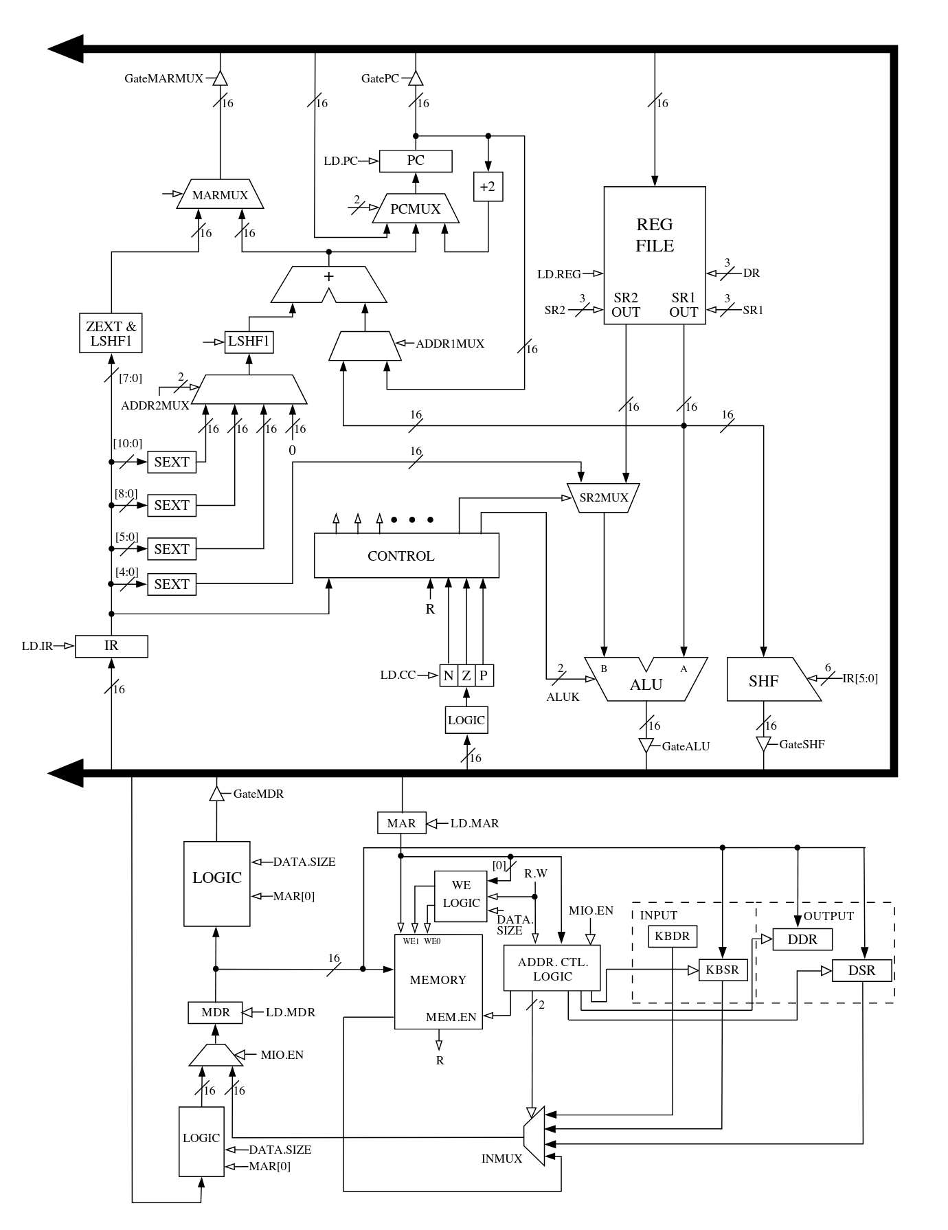
All combinational datapath elements are modeled as pure Go functions. This includes:
- Multiplexers (MUXes)
- Sign and zero extenders
- The shifter
- The ALU
These components take their inputs and control signals and immediately produce outputs, mirroring how combinational logic behaves in real hardware.
In contrast, sequential elements such as registers and memory are modeled with explicit clock behavior. State updates occur only on simulated clock edges (rising or falling, depending on the element), which enforces correct ordering and prevents illegal state transitions. This distinction turned out to be critical for avoiding subtle bugs where state appeared to update too early.
Register reads are treated as combinational, allowing instruction logic to observe register values within the same cycle, while writes are deferred until the appropriate clock edge. This closely mirrors how register files behave in real processors.
Finite State Machine (FSM)
Instruction execution is driven by a microcoded finite state machine, also derived from the LC-3b control FSM presented in Appendix C of Patt and Patel.
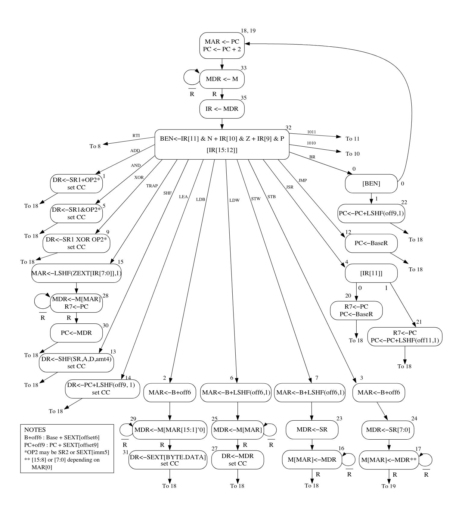
Rather than hard-coding control flow with large switch statements, the FSM is implemented as a “microcode” table represented by a Go map:
- Key: current microinstruction (state)
- Value: a struct containing:
- Control signals for the datapath
- Logic for selecting the next microinstruction (COND, Jump, MemReady)
Each microinstruction describes what the datapath should do for a single cycle - which registers to load, which MUX paths to select, whether memory is accessed, and how the program counter is updated.
At runtime, the simulator:
- Fetches the current microinstruction
- Applies its control signals to the datapath
- Evaluates any conditionals (e.g., instruction opcode, condition codes, memory readiness)
- Transitions to the next microinstruction accordingly
This approach closely mirrors how real microcoded control units work and it made it significantly easier to reason about instruction execution at a cycle-by-cycle level.
Why This Approach Worked Well
Modeling the datapath and control logic separately helped enforce a clean architectural boundary between data movement and control flow. The datapath remains largely generic, while the FSM defines when and how each component is used.
This design also made debugging more manageable. Once I got the timing sorted out, when incorrect behavior occurred, it was usually possible to narrow the issue down to either:
- A faulty datapath element (e.g., incorrect sign extension), or
- An incorrect control signal or state transition in the FSM
Overall, implementing the LC-3b this way provided a much deeper understanding of how real CPUs orchestrate work across multiple cycles - far beyond what is visible from the ISA alone. Which leads me to the next section.
Things I Learned / Hardships
This project was a deep dive into how abstract hardware concepts translate into concrete software behavior. While the simulator itself is relatively small, building it forced me to confront many of the same design constraints and tradeoffs that exist in real processors.
A few key takeaways from the project:
-
A CPU is fundamentally a large state machine.
At its core, instruction execution is nothing more than a carefully orchestrated sequence of state transitions. Once the datapath is correct, most of the complexity lives in when things happen rather than what happens. -
Microarchitectural performance metrics became tangible.
Concepts like cycles per instruction (CPI), instruction counts, and memory access frequency can feel abstract when encountered in lectures or textbooks. Implementing a profiler forced me to explicitly define what constitutes a “cycle” and when one should be counted. Seeing CPI change as different instruction mixes executed made these metrics intuitive in a way that static examples never did. Frequent memory access is a real performance killer.💡Foreshadow to caching which I’ll be learning soon 🙂 -
Memory behavior is more nuanced than it initially appears.
Implementing memory access logic exposed the importance of word alignment and address calculation. Since the LC-3b is byte-addressable but often operates on 16-bit words, correctly handling word-aligned accesses and understanding what it means to extract or store individual bytes required careful attention. This made it clear how much work an ISA specification quietly delegates to hardware, and how easy it is to get memory semantics subtly wrong. -
Proper sign extension.
Many LC-3b instructions operate on immediate values encoded directly in the instruction word. For example, an instruction like
ADD R1, R1, #-1encodes-1as a 5-bit immediate value0b11111. In the LC-3b, that value must be sign-extended to 16 bits before being used by the ALU.If sign extension is implemented incorrectly, arithmetic will often still “work” at a superficial level but produce subtly wrong results. These bugs tend to fail silently and can be extremely difficult to debug later in execution. Don’t ask me how I know…
In my implementation, I chose to represent all architectural values using unsigned integers, mirroring how hardware fundamentally treats data as raw bit patterns rather than signed numbers. While this aligned well with my mental model of real hardware, it introduced a few non-obvious challenges in Go.
Although Go correctly performs binary addition on unsigned integers (e.g.,
0b01 + 0b11), the language does not inherently interpret those values as two’s complement signed numbers. As a result, operations that assume signed semantics, such as interpreting an immediate as negative, required explicit bit manipulation to correctly extend and preserve the sign.Another consequence of using unsigned integers was the lack of support for arithmetic right shifts, which are only defined for signed integers in Go. Since arithmetic shifts are important for preserving sign bits, I had to implement custom logic to emulate this behavior when needed.
💡I created a bitmask with logical shifts and bitwise OR’d it to the int that needed to be sign extended
In my opinion, the hardest part of the project wasn’t writing the code - it was learning to think the way the hardware thinks. Modeling behavior at this level forces you to reason about time, state, and side effects explicitly, and it provided a much deeper understanding of how real CPUs actually execute programs.
What’s Next?
There are plenty of ways this simulator could be extended:
- Adding pipelining or out-of-order execution
- Writing an assembler/disassembler for LC-3b to make it easier to play around with
- Building a step-through debugger or visualization tool
- Modeling cache or memory hierarchy behavior
Overall, this project was a great way to solidify my understanding of computer architecture and low-level systems design.